
Plasma Spray Coating vs. Magnetron Sputtering: Which Process Is Right for Your Application?
No, they are not the same. Both processes use plasma, and both can deposit ceramics, which is why the names often get mixed up in tenders, RFQs and even purchase orders. Beyond that, they work in completely different ways, produce very different coatings and solve very different problems.
Buyers and plant engineers often come across sputtering in a datasheet or research paper and wonder if it can replace thermal spray on their parts. Having run plasma spray systems since 1984, here is how we explain the difference.
Why the Two Get Confused
The common word is “plasma”. In both processes, a gas such as argon is energized until it ionizes. What happens next is where they part ways.
In plasma spraying, the plasma is a heat source. In sputtering, the plasma is a source of ions that act like tiny hammers. One melts material; the other chips it away atom by atom. Add the fact that both can lay down alumina or other oxides, and it is easy to see why the terms get swapped.
You may also see “RF plasma spraying” or “induction plasma spraying” in technical papers. That is a variant of thermal spray that uses a radio-frequency torch, and it is still a different process from RF magnetron sputtering.
How Plasma Spray Coating Works
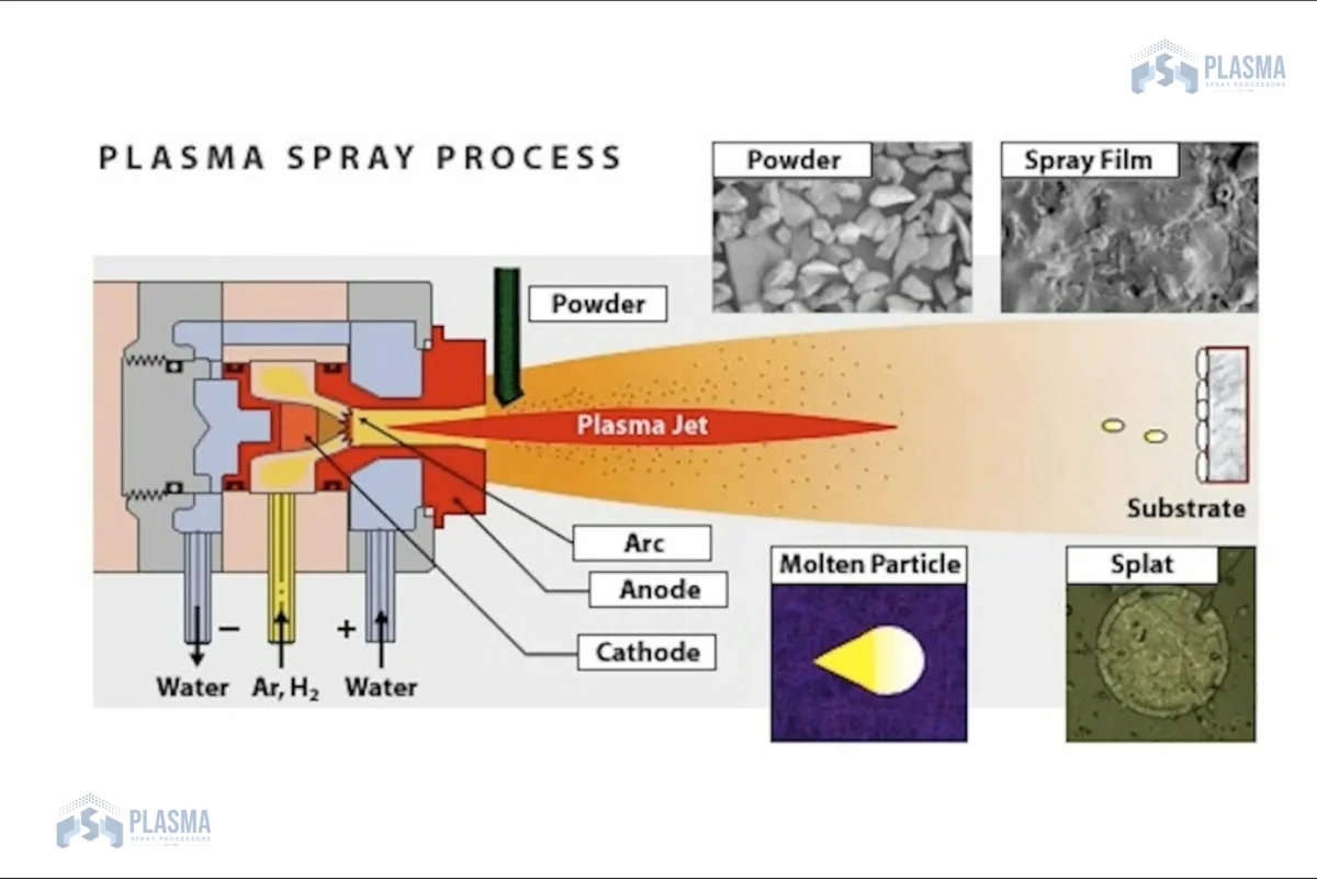
The coating builds up in layers. Our plasma spray coating systems typically apply aluminum oxide, chromium oxide, zirconium oxide and metallic alloys at thicknesses between 50 and 500 microns. Because the work happens in open air, part size is rarely a barrier. Long steel mill rolls, pump sleeves and turbine parts are all routine jobs.
The coating is then ground or polished to final size. This makes plasma spray suited to rebuilding worn parts, not just protecting new ones.
How RF Magnetron Sputtering Works
Sputtering is a physical vapor deposition (PVD) process carried out in a vacuum chamber. A solid plate of the coating material, called the target, sits opposite the part, called the substrate.
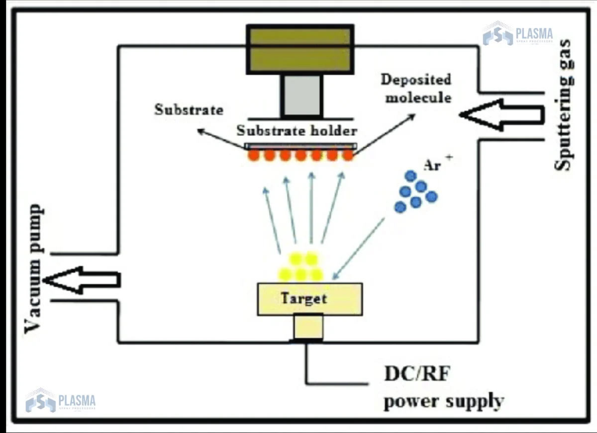
Argon is let into the chamber at very low pressure and turned into plasma using radio-frequency power. Positive argon ions slam into the target and knock atoms loose. Those atoms travel across the chamber and condense on the substrate, growing a film one atomic layer at a time.
Two details explain the name:
- RF (radio frequency) power is used because it can sputter insulating targets such as oxides. With plain DC power, charge builds up on an insulating target and the process stalls.
- Magnetron refers to magnets placed behind the target. They trap electrons close to its surface, which makes the plasma denser and the sputtering faster.
The result is an extremely thin, smooth and uniform film. Sputtering suits semiconductor wafers, optical coatings, thin-film solar cells, sensors and similar precision work. The part has to fit inside the chamber, and deposition is far slower than thermal spray.
Side-by-Side Comparison
| Feature | Plasma Spray Coating | RF Magnetron Sputtering |
|---|---|---|
| Environment | Open air (atmospheric) | Vacuum chamber |
| Starting material | Powder | Solid target |
| How material arrives | Molten droplets | Individual atoms |
| Typical thickness | 50 to 500 microns | Nanometers to a few microns |
| Bond to surface | Mechanical, on a grit-blasted profile | Atomic-level adhesion on a clean surface |
| Part size | Very large parts possible | Limited by chamber size |
| Rebuilds worn size | Yes | No |
| Typical use | Wear, corrosion, heat, restoration | Electronics, optics, functional films |
Which One Does Your Part Need?
Start with the job the surface has to do, not the name of the process.
If a roll is scoring, a sleeve is eroding, a seal face is corroding or a part has lost size, you need thickness and toughness. A sputtered film a micron or two thick would wear through quickly in that kind of service. Plasma spray, HVOF or another thermal spray method is the right family to look at.
If you need a precise optical, electrical or barrier layer on a wafer, lens or glass panel, thermal spray is far too thick and rough. Sputtering or another PVD process is the right route. That work is done by specialist thin-film facilities, not thermal spray shops like ours.
There is some overlap in high-tech sectors. In semiconductor manufacturing, for example, the chip is built using sputtering inside the tool. The chamber parts themselves often need thick plasma-sprayed ceramic coatings to resist plasma erosion.
Not Sure Which Process Fits?
We have more than 40 years of experience in thermal spray, ISO 9001:2015 and AS 9100:2016 certification, and USA and German coating systems. We help plants across India pick the right coating for wear, corrosion and heat problems. If your part is better suited to sputtering, we will tell you that plainly.
Contact our team with your drawing or part details for a free consultation.